Browse categories
English
$
USD
Connect to your AI
ESP32 PCB and IoT Hardware Designer, Custom PCB, KiCad and Wireless Solutions
Need an ESP32 PCB designed professionally in KiCad?
I will design your custom ESP32 PCB in KiCad, from schematic and component setup through PCB layout, routing, and manufacturing-ready files.
What you can get:
Whether you have an existing schematic, circuit diagram, reference design, or project requirements, I can turn your ESP32 concept into an organized KiCad PCB suitable for prototyping or manufacturing.
Please provide your circuit, ESP32 module, components, board dimensions, interfaces, power requirements, or reference files before ordering.
Let's build your ESP32 PCB in KiCad.
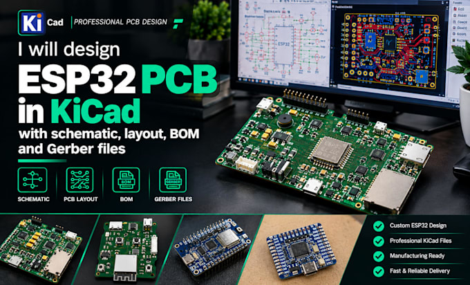
Can you design an ESP32 PCB specifically in KiCad?
Yes. This gig focuses on custom ESP32 schematic and PCB layout development using KiCad.
Can you convert my ESP32 schematic into a KiCad PCB layout?
Yes. You can provide your existing schematic or circuit, and I can develop the corresponding KiCad PCB layout.
Will I receive the editable KiCad project files?
Yes. Editable KiCad project/source files can be included according to the package you select.
Can you provide Gerber, drill and BOM files?
Yes. Depending on the selected package, I can provide BOM, Gerber files, drill files and other manufacturing deliverables.
Can you check my ESP32 KiCad PCB before manufacturing?
Yes. The appropriate package can include basic DRC/ERC and design checks to help identify common PCB design issues before manufacturing.
