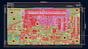
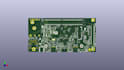
This gig is ideal for products requiring High-Speed Digital Interfaces, complex BGA/LGA routing, controlled impedance, and precise signal timing. Every PCB is designed with careful attention to Signal Integrity (SI), Power Integrity (PI), EMI/EMC compliance, thermal performance, and Design for Manufacturing (DFM) to ensure smooth fabrication and assembly.
What I Offer:
- High-Speed PCB Layout
- Schematic Capture
- 2 to 32 Layer PCB
- Multi-Layer Stack-up Planning
- Controlled Impedance PCB
- Differential Pair Routing
- Length Matching and Timing Optimisation
- Signal Integrity and Power Integrity Considerations
- BGA, LGA, QFN, QFP, CSP, and Fine-Pitch Component Fan-Out
- HDI PCB Design with Blind and Buried Vias
- Via-in-Pad and Microvia Routing
- DDR3, DDR4, DDR5 and LPDDR Memory Routing
- PCIe Gen3, Gen4 and Gen5 PCB
- USB 2.0, USB 3.2 and USB Type-C
- HDMI, DisplayPort, Ethernet, MIPI CSI/DSI and SATA
- FPGA and High-Speed Processor PCB Layout
- RF and Mixed-Signal PCB
- Power Supply and DC-DC Converter Layout
- Design Rule Check (DRC)
- Design for Manufacturing (DFM)
- Design for Assembly (DFA)
- Component Placement Optimisation
- Thermal Management & Copper Balance