Browse categories
Explore
Fiverr Pro
English
$
USD
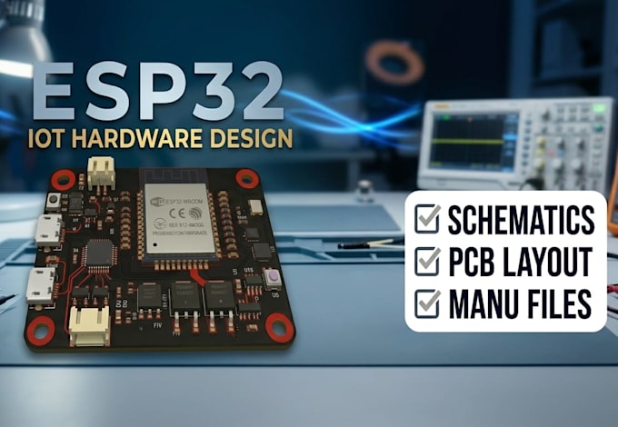
Turn Your ESP32 Prototype into a Production-Ready Product!
Ready to scale your breadboard setup? Don't risk signal drops or power failures with generic layout technicians. I engineer custom, high-performance embedded hardware from absolute scratch (Schematic + Layout).
What I Do:
What You Get:
Please message me with your project details or a simple block diagram before placing an order so we can align on your goals.


_p6jlxz.jpg)

Do you design the schematic from scratch, or do I need to provide one?
I design everything from scratch! You do not need a pre-made schematic. You only need to provide a block diagram, a list of components you want to use, or simply a text description of your project's features. I will handle the engineering, component selection, and layout.
Are the native design source files included in the price?
Yes, absolutely. Unlike many sellers who charge extra for them at checkout, you receive the full native project source files (Altium Designer or KiCad) in every single package tier with zero hidden fees. You own 100% of your intellectual property.
Will my board files be ready for automated factory assembly (SMT)?
Yes. Every delivery package includes a production-ready manufacturing kit tailored for houses like JLCPCB, PCBWay, or Mouser. You will receive standard Gerber files, NC Drill files, a Pick-and-Place matrix (CPL/Centroid), and an active Bill of Materials (BOM) with exact manufacturer part numbers.
Can you design the PCB to fit a specific custom plastic enclosure?
Yes. If you have a specific housing or case, please provide a 3D STEP model, a DXF layout file, or a dimensioned drawing. I will map out the exact board dimensions, mounting holes, and edge-connector placement so your custom board fits flawlessly.
What happens if the fabrication house flags an issue with the design?
I design strictly to your chosen manufacturer's DRC (Design Rule Check) specifications to prevent issues. However, if a fabrication house flags an assembly layout conflict or component clearance issue, simply message me. I will modify the layout files immediately under your project revisions.